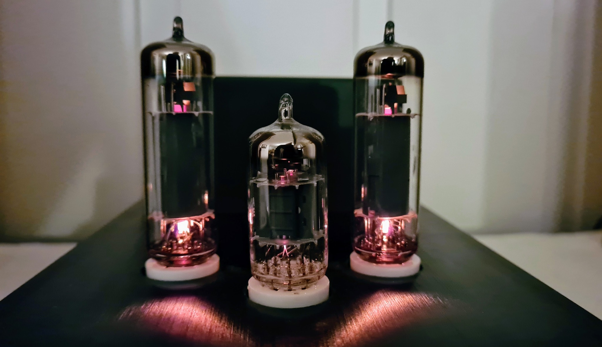
Tuning indicator tubes have hardly been manufactured the last 50 years, and some types are scarce, e.g. the 6U5. When restoring a Tandberg Sølvsuper 4 some months ago, I was lucky to acquire a mildly used 6U5 to replace the burnt out one; for a reasonable price. For the next Sølvsuper 4 restoration, I started looking for alternatives.
One of my previous projects was making a OLED-based replacement for EM84 which looks reasonably authentic. The circular shape of the 6U5 makes it more challenging to mimic than the rectangular EM84. Others have come up with solutions involving spinning LEDs or circular LED matrixes, but I thought I’d try a different approach to make it look more realistic.
Since the introduction of smart watches, an increasing number of round displays have become available on the market, most of which are too large to fit inside the glass envelope of a tube which has an outer diameter of less than 3 cm, and finding a suitable display and learning how to interface it, was probably the most challenging tasks of this project.

The only candidate I could find was a 0.99″ IPS panel with GC9107 driver, SPI interface, and 12-pin FFC connector, at Buydisplay.com. Apparently, no breadboard-friendly display modules incorporating this panel had been made before; at least I couldn’t find any for sale, so before starting prototyping, I had to design and manufacture an interface board.

The picture shows the homemade display interface board, controlled by a DIY ATMEGA328P development board, running a basic “Hello World” test code, utilizing the versatile Arduino GFX Library.
I quickly learnt that the old ATMEGA328P (AVR, 8-bit, 16MHz) was too slow for creating responsive graphics with this display, which has a resolution of 128×115 pixels.
Instead, I chose a STM32F103CBT (ARM, 32-bit, 72MHz), which is a mainstream MCU at the lower end of the STM32 family, but which proved to be sufficient for this task.
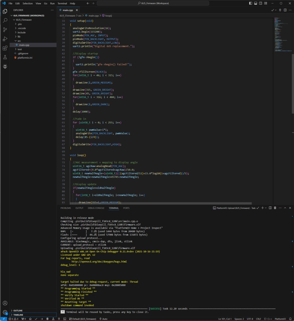
Firmware is written in C/C++ with Arduino framework. The IDE is PlatformIO on VS Code.
The electronics hardware is implemented on two PCBs:
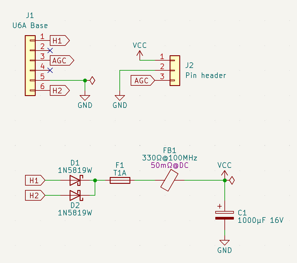
The first board is a circular base which fits inside the U6A socket, and which receives filament voltage from the radio. The circuit contains half-wave rectifier, reservoir capacitor and fuse, plus a ferrite bead to filter out RF noise from the MCU board, and which might otherwise affect the radio via the heater supply.
This board also receives AGC voltage from the radio, which is proportional to the received signal strength.

Conditions for the circuit to work:
- In the radio, the magic eye’s cathode (pin 5) must be connected to ground.
- One wire of the heater supply must also be connected to ground. This can be either pin 1 or 6.
Most radios implementing 6U5 are expected to meet these prerequisites, but some might not. The radio used during development is Sølvsuper 4.
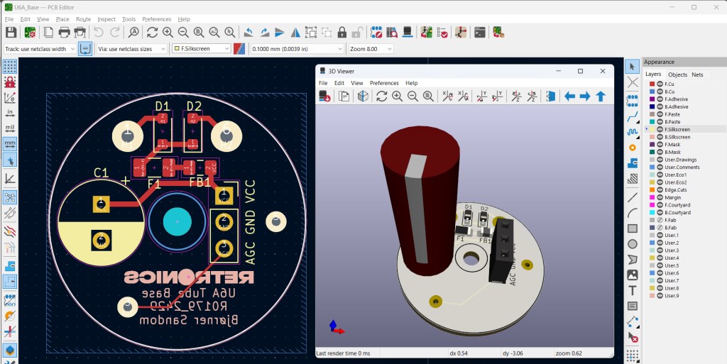
PCB design in KiCad.
The MCU board is where the magic takes place (click for high resolution):
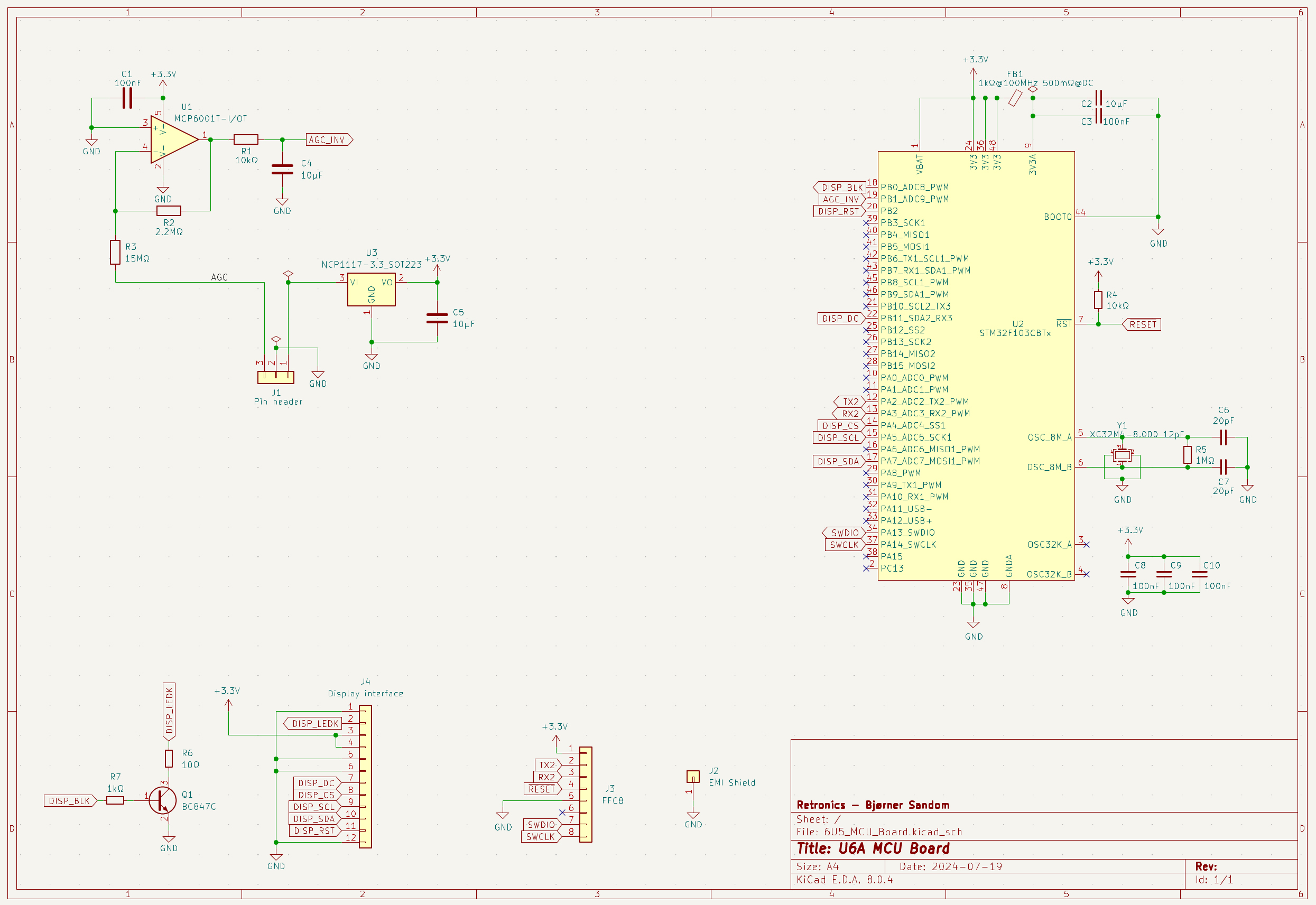
This circuit receives unregulated DC supply voltage from the base board (around 8 volts). This is regulated to 3.3V for the MCU and display by an NCP1117 LDO. The AGC voltage from the radio is expected to vary between 0 and -22 V (with respect to GND). This has to be translated to a a positive voltage between 0 and 3.3V, a task that is performed by an inverting amplifier stage. The MCP6001 OP AMP is selected because it works rail-to-rail on both input and output, with such low supply voltage as what’s used in this circuit, and because it has a very high input impedance (1013Ω || 3pF). The input resistance of the stage = R3 = 15MΩ, and it needs to be this high to minimize impact on the radio’s AGC voltage. On the amplifier stage’s output, there is an RC low pass filter (R1 and C4), with a cut-off frequency of 1.6Hz. The inverted, reduced and filtered AGC voltage is fed into an A/D-converter input of the STM32 microcontroller, where it is digitized and filtered by firmware. Using an 8MHz crystal for the clock of a 72MHz MCU may look confusing, but the frequency is scaled up by some magic inside the STM32 (PLL). The MCU controls the aforementioned display panel via SPI bus (+ some extra control lines), and the physical interface towards the panel is a 12-pin FFC connector with 0.5mm pitch. An 8-pin FFC connector interfaces an ST-LINK adapter during programming and debugging. A single BJT transistor (Q1) drives the backlight LED of the display, and is controlled by a PWM signal from the MCU, with gradually increasing duty cycle during the first seconds after power-on, to make the display fade in, almost like what an original 6U5 tube would do, but I chose to make it a little faster.

PCB design in KiCad. An EMI shield is preventing noise from the MCU, crystal and surrounding circuitry, from affecting the radio reception.
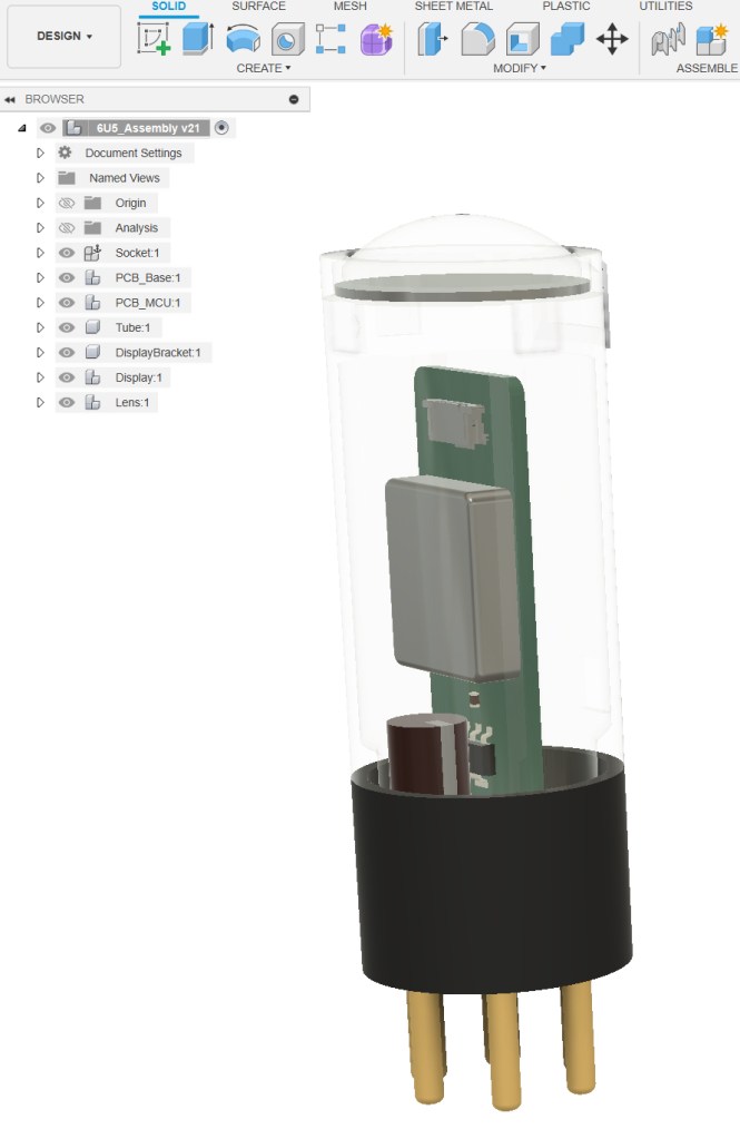
3D renderings are shown with and without this shield, to illustrate component placement.
I sent the fabrication files to jlcpcb.com for PCB manufacturing, but soldered all components manually.
A good 3D-modeling software is indispensable when planning the assembly and designing parts for 3D printing. I prefer Fusion360, a professional modeling software which is free for personal use.
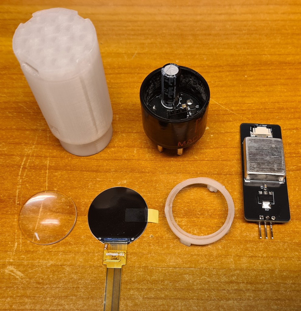
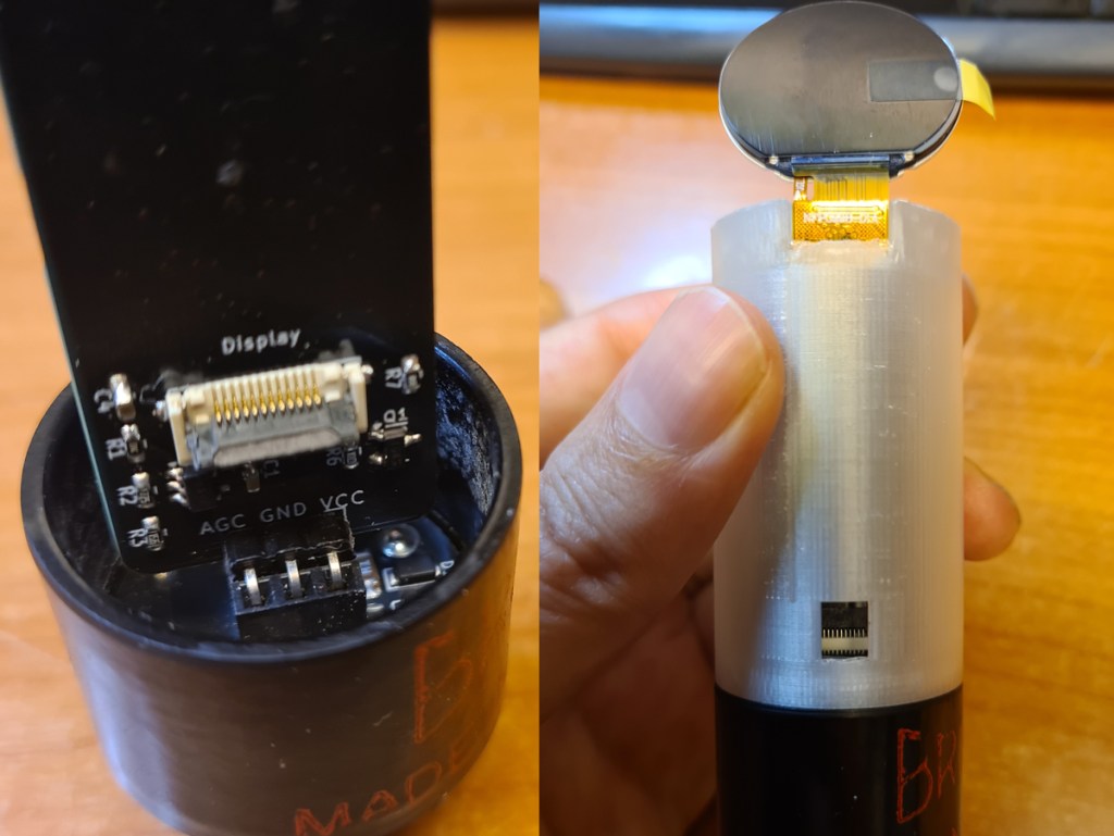
The parts in this design are U6A tube socket (which will be reused from a burnt-out 6U5), and inside it is the circular base PCB with rectifier and connectors. On top of this, the MCU PCB is mounted. The circuitry is covered by a plastic tube, on top of which the display panel and the lens is fastened with a plastic bracket.
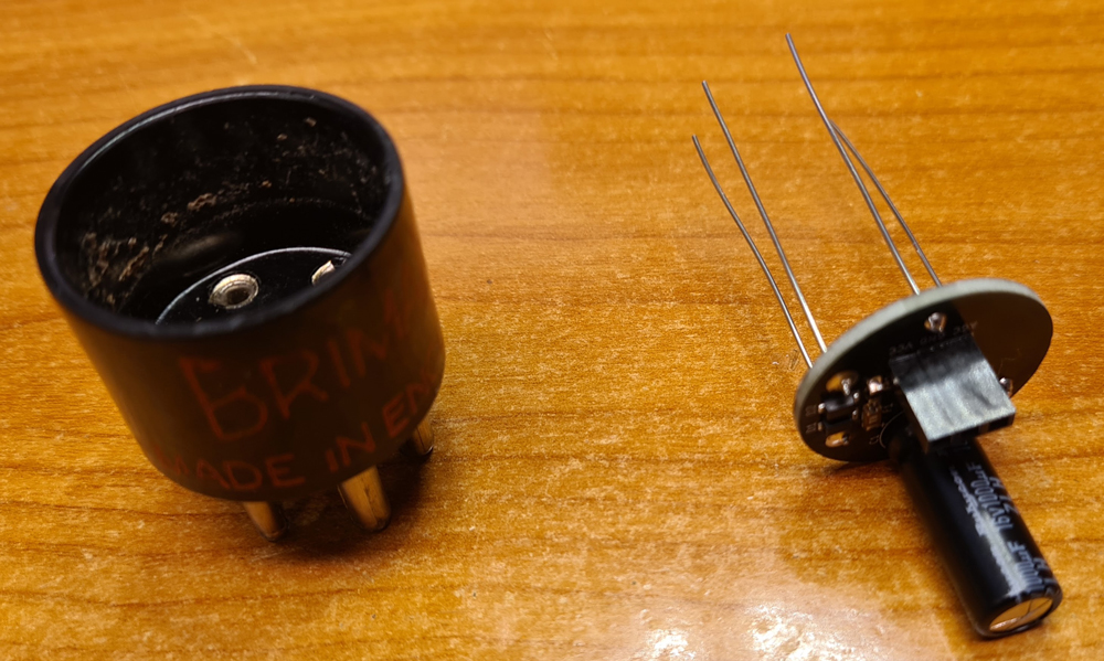
The finished base PCB, ready to be inserted into the U6A socket of a burnt-out 6U5. I had to break the glass of the original tube to get it out of the socket. If you are doing so, I recommend putting the tube inside a plastic bag before hitting it with a hammer, and using both safety glasses and gloves.
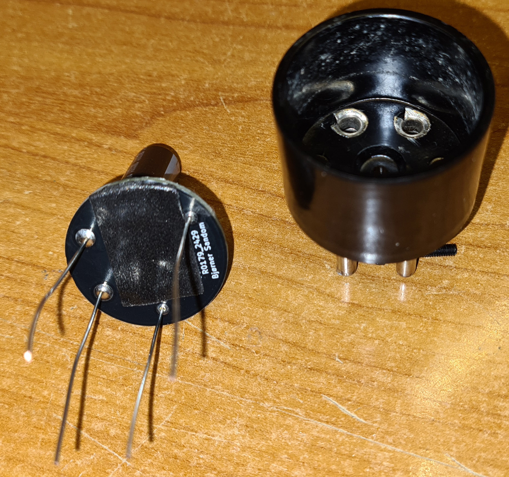
When used in a radio receiver, there will be fairly high voltages (around 250V) on pins 2 and 4. These pins are not utilized in the digital 6U5, but they need to be insulated from the PCB. I used a piece of double-sided foam tape for this. It also keeps the PCB in place when soldering the wires inside the socket pins.
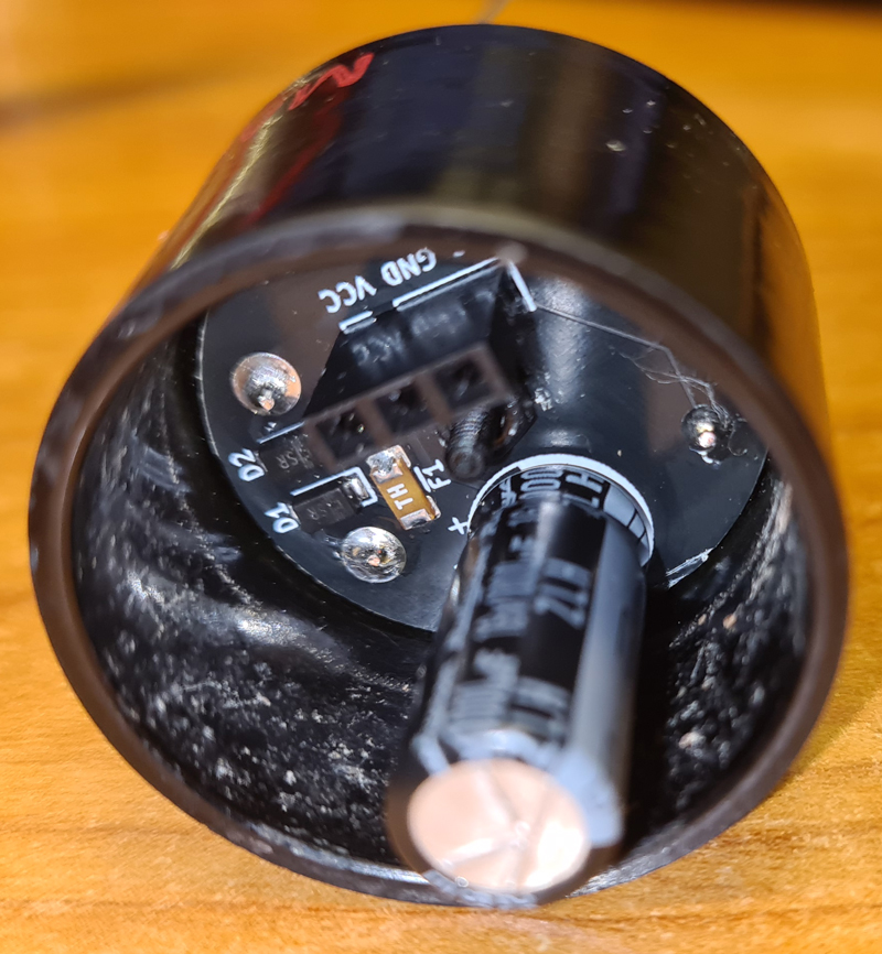
Make sure to get the orientation correct. The wires next to the diodes go inside the two thicker pins of the socket. These are used for filament voltage supply.
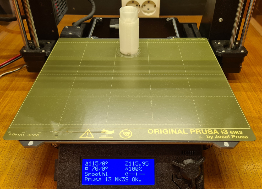
My trusty old Prusa MK3S+, still going strong. The plastic parts are printed with translucent ABS, but other materials like ASA or PETG will do just fine.
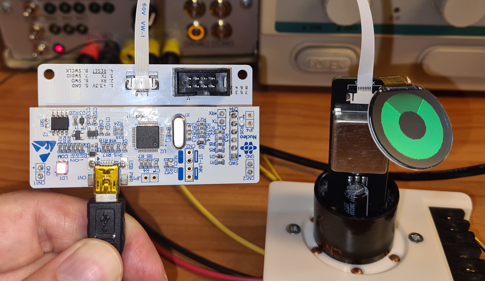
Firmware upload and testing via ST-LINK before assembly. The ST-LINK adapter is reused from a Nucleo development board and extended with a DIY interface board, in this case connected via a 8-pin FFC cable.
The 6U5 unit is powered with 6.3VAC from a homemade PSU for experimenting with vacuum tubes.
The 6U5 test adapter is also homemade.
Thread the display cable through the slot in the tube, all the way down to the display connector of the MCU board. This is accessible via a small window in the tube. Use a small screwdriver to carefully lock the FFC-connector.

Put the lens on top of the display and lock it in place with the 3D printed display/lens bracket. No glue is needed. The display cable needs to be bent at a sharp angle, but it’s not likely to break. During design and testing, my display has been in and out of the tube at least a dozen times without breaking.
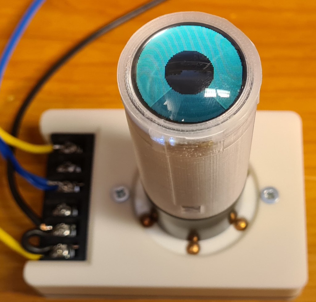
In a closeup photo, you can see that the graph is built up by pixels, but in practice the unit looks almost analog.
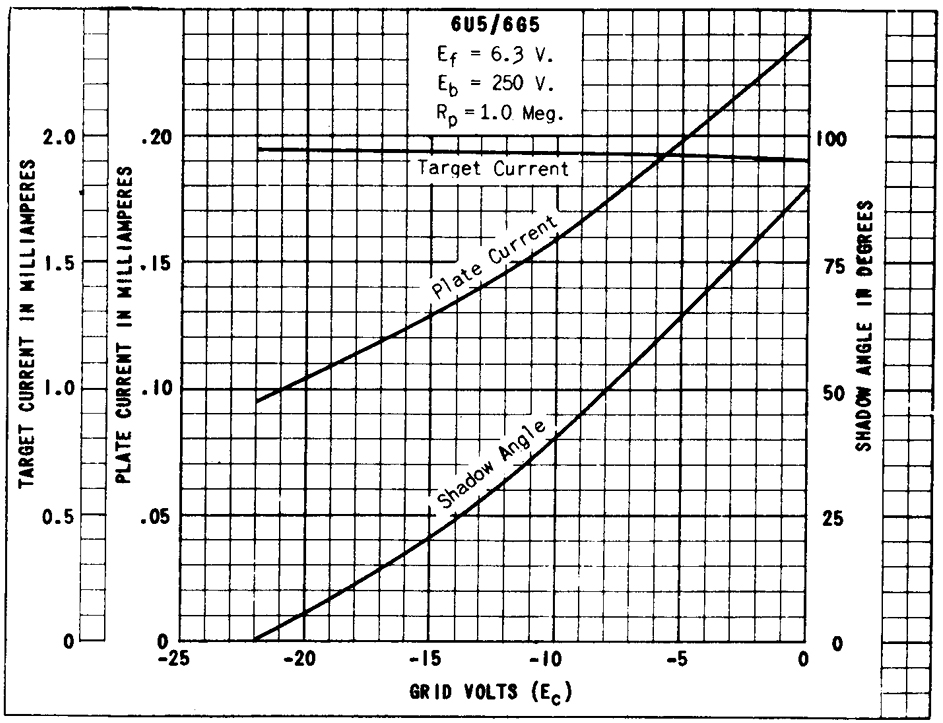
From datasheet: shadow angle as a function of gate voltage, when supply voltage is 250V and load resistor is 1MΩ. In the Sølvsuper 4 radio and in the test setup, the tube operates under the same conditions.
Replicating this curve in a digital solution, while simultaneously filtering out noise, and keeping a fast response was challenging, but this is the algorithm I came up with:
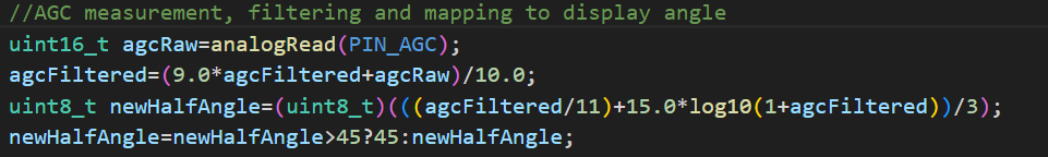
The AGC voltage (0 to -22) is transformed to a voltage between 0 and +3.3V by hardware (the inverting amplifier stage on the MCU board). A 10 bit A/D-converter on the STM32 transforms this to a value between 0 and 1023, retrieved to the agcRaw variable by the analogRead() function. Noise on the AGC line could cause the display to flicker. To avoid this, there is filtering both in hardware (RC filter on the OP AMP output) and in firmware. The variable agcFiltered is calculated as a kind of moving average; the weighted average of previous average calculation and the new raw value, in a ratio of 9 to 1. Next mapping between filtered AGC value and shadow angle is calculated as a weighted average between linear mapping and logarithmic mapping, with emphasis on the linear.
When putting high frequency digital circuitry inside an analog radio receiver, particularly AM, RF noise affecting the radio reception is a concern. The solution contains a microcontroller clocked by a 8MHz oscillator, scaled up to 72MHz by PLL. Therefore the MCU and surrounding circuitry is shielded between an aluminium box and a grounded copper layer on the PCB. The display cable is unshielded, and carries an SPI bus signal clocked at 1.8MHz. This bus carries data every time the display is updated (every time the shadow angle is to be changed due to variations in the AGC voltage), but is otherwise quiet.
The display backlight is controlled by PWM pulses, but this is clocked at 1kHz, and is not likely to cause any trouble, as the amplitude of the harmonics at 140kHz (the radio’s lower end of the LW band) and upwards, will be minimal.
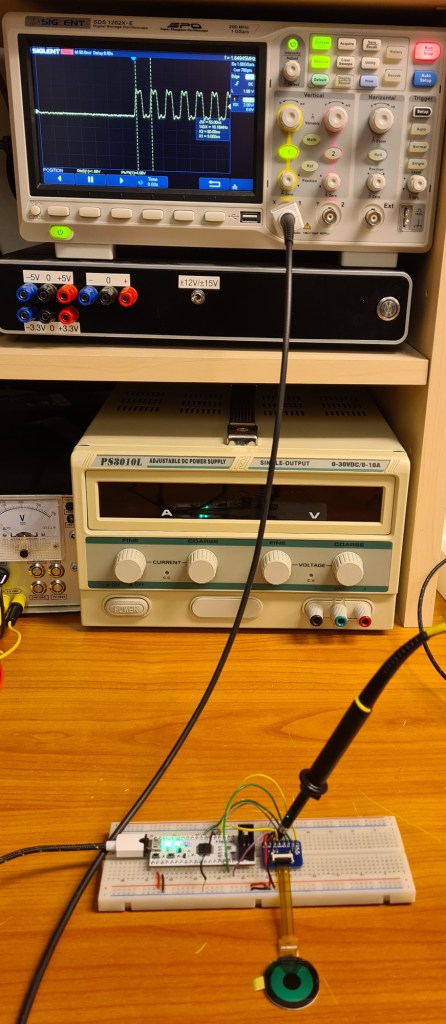
Therefore, the SPI data bus is my main concern when it comes to noise. To the left, the SPI clock is shown on an oscilloscope. Don’t worry about the ringing, as this mainly caused by inductance in my lousy breadboard wiring.
In lack of fancy test gear for measuring RFI, I tested the digital 6U5 inside the radio in which it will be used, a Sølvsuper 4. The method was simply sweeping through all radio’s bands and listen for noise through the loudspeaker. In a modern world with noisy electronic gadgets everywhere, especially those containing switch mode power supplies, the air is full of radio interference. I’ve tried turning off most sources of noise in my own house, but I did not attempt to cause power outage to the neighbors’ houses to achieve radio silence. Instead I temporary added a power switch to turn the digital 6U5 on and off, to check if that affected the noise.
To keep the SPI bus busy at all times, I disconnected the 6U5 from the radio’s AGC line, and instead fed the AGC input of the tube with a 1Hz signal from a function generator. This is what causes the continuous waves on the display.
The digital 6U5 in practice. It was hard to get a good video, and the tube looks better in real life, but at least this video gives some impression:
The signal comes from a DIY radio transmitter.
All PCB design files (KiCAD), fabrication files (gerber), 3D models (.stl) and code (C++, PlatformIO) are shared on Github, for personal use only; not for commercial use / sale of neither the complete solution nor parts of it.

Leave a reply to OTA: Modern “Magic Eye” Tuning Tubes, Multi-Radio SDR On-The-Move, Faster SatDump, and More – MyriadRF Cancel reply