If you are soldering the components in a traditional way, using soldering iron, I recommend starting with the PSU + either USB connector or pin headers for VIN, 3.3V and GND, and verify that the buck converter delivers correct output voltage, before soldering MCU and other components.

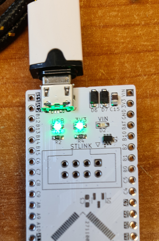
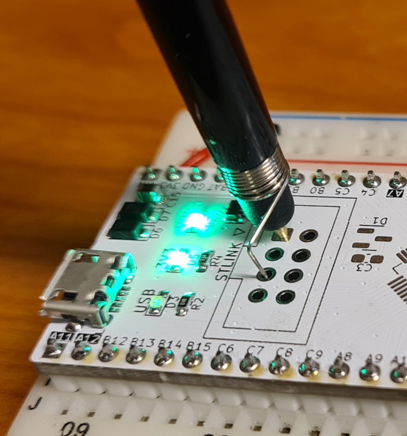
The easy test: Connecting USB power from a computer or cell phone charger and measuring output voltage between pins 3V3 and GND, with a multimeter. My board delivers 3.32V, which is pretty much spot on.
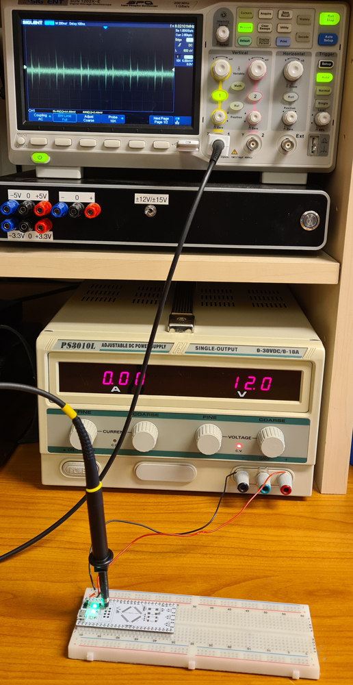
I did some extra measurements with and without load, to check the performance of the buck regulator circuit. The power source is a linear lab PSU with 12V output voltage, connected to pins VIN and GND.
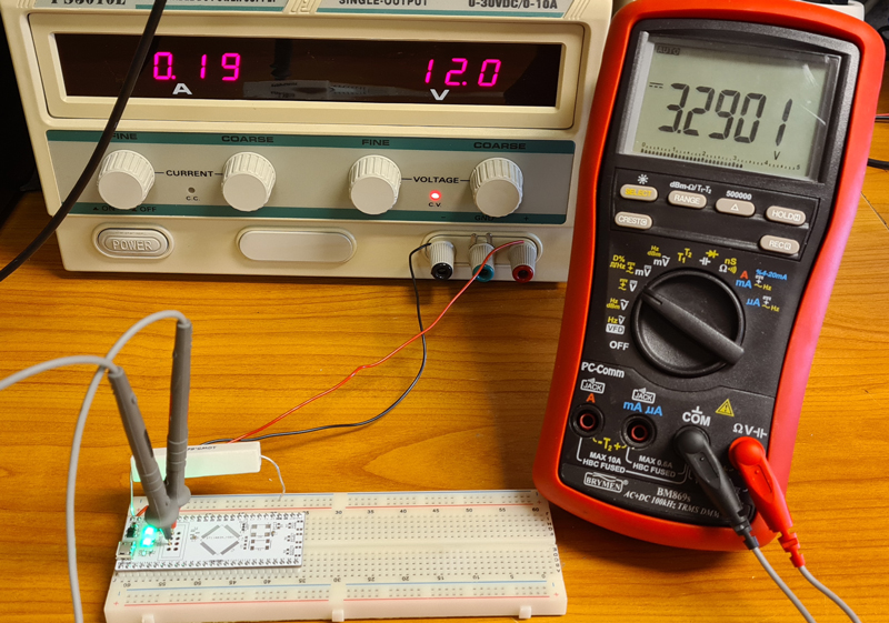
Load test: A 5.6Ω resistor is connected between 3V3 and GND, to draw about 580mA (slightly less than the TPS560430s max rating of 600mA.
The output voltage only drops to 3.29V, which shows that the PSUs load regulation is good.


With the PSU confirmed to be working well, it’s time to solder the rest of the components. I desoldered the STM32 from the Nucleo board, and reused it on the new board.
When soldering the microcontroller’s LQFP64 package, a microscope may be handy. I’m using a modified version of Andonstar 407.

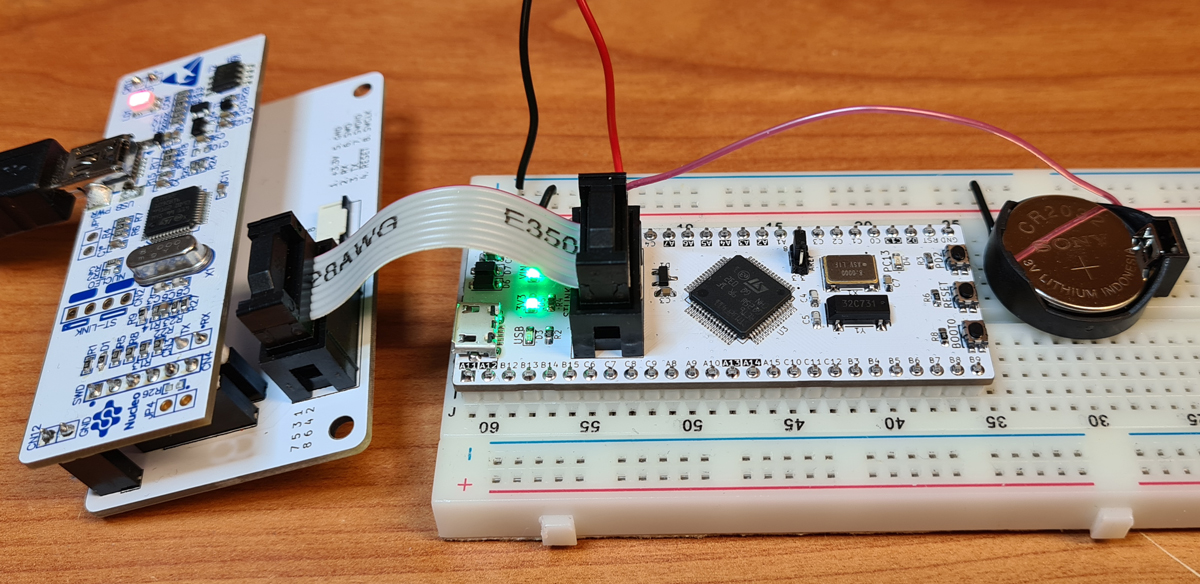
Though it’s possible to program the WhiteBoard64 via USB, my preferred programming and debugging interface is ST-LINK. Nucleo boards come with a semi-integrated ST-LINK adapter which can be separated from the main board. I made an interface board which makes connection to the WhiteBoard64 (and all my other STM32 based projects) quick and easy.
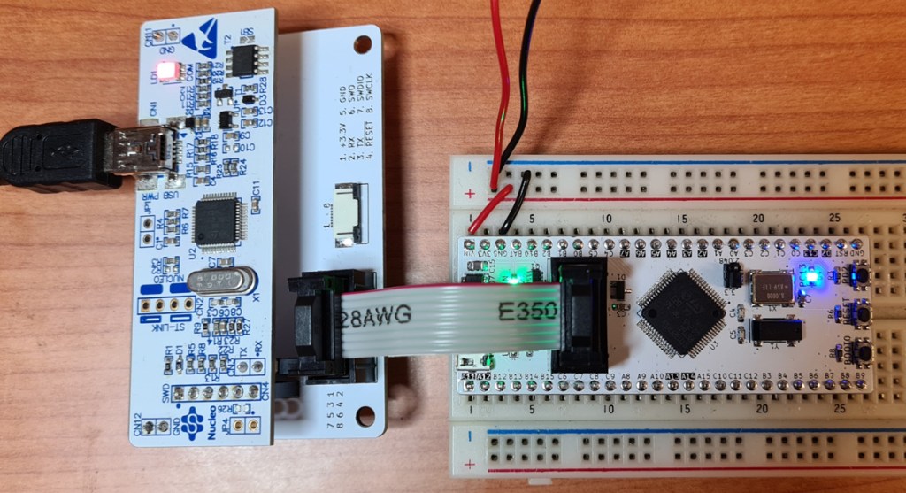
Nucleo-based ST-LINK adapter, connected to the WhiteBoard64 via 8-pin IDC cable.
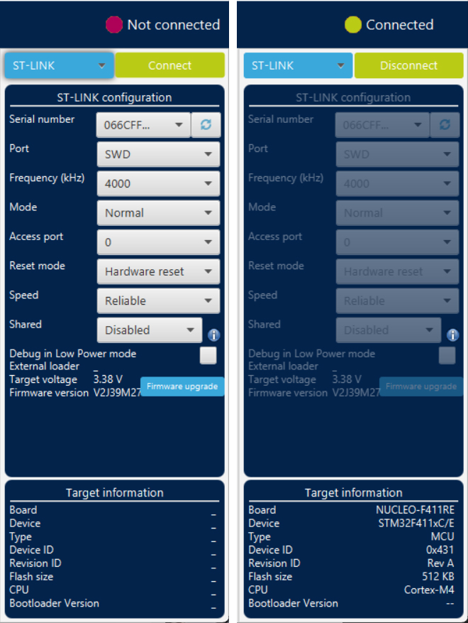
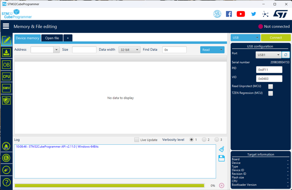
Testing the ST-LINK interface in CubeProgrammer.
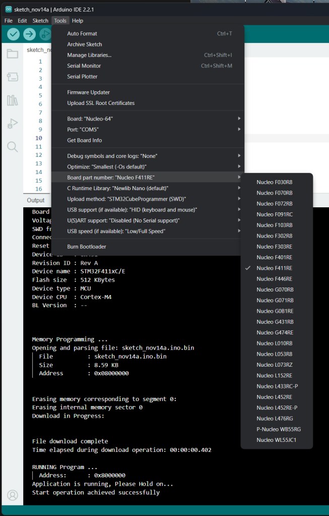
For hobbyists, Arduino IDE is probably the most commonly used development software, and you may program the WhiteBoard64 from this IDE, given that you’ve installed the board definitions for STM32 boards. Select Board Part Number: Nucleo F411RE if you are using the STM32F411RET6 microcontroller, and Upload method: STM32CubeProgrammer (SWD) if you are using an ST-LINK interface adapter.
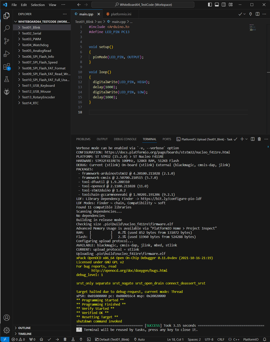
If you are making more advanced projects, you have probably already moved on to a better development environment. Personally, I prefer using VSCode with PlatformIO. For Arduino IDE users, PlatformIO may be a little confusing at first, but once you get used to it, you don’t want go back to Arduino IDE, except maybe for small test sketches. You’ll find lots of tutorials on YouTube on how to get started with PlatformIO. Professional STM32 programmers will probably use STM32CubeIDE, but that IDE is only for ST microcontrollers, while PlatformIO supports most modern microcontrollers.
I’ve posted a few program examples for WhiteBoard64 on GitHub. These are also listed in the left column of the screenshot above.
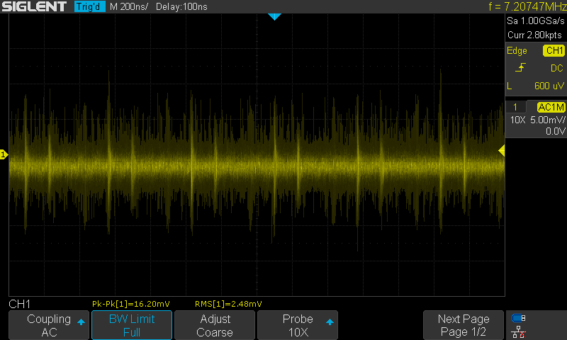
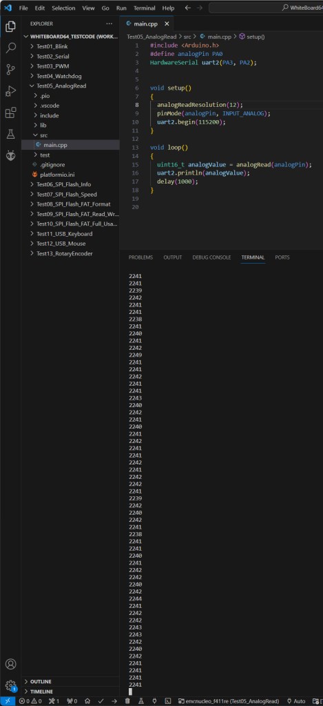
One concern when using a switched voltage regulator as supply for a microcontroller, is that switching noise/ripple may affect ADC accuracy. I’ve done some tests:

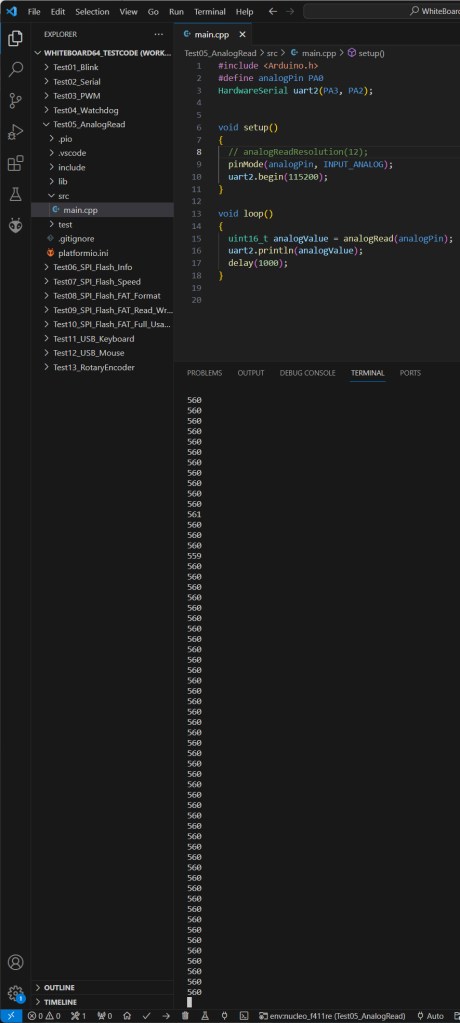
The program performs 1 measurement per second, and writes the result to console.
At 10 bit ADC resolution, the results varies with +/- 1 LSB, which is pretty good for an MCU driven by a switched regulator. If the regulator is simultaneously used to power other devices with variable current draw, this will affect the results.
If I use 2.048V reference instead of the filtered 3.3V, the variation is still +/- 1 LSB. This reference, however, stays at the same voltage, regardless of other devices drawing current from the switched regulator.
With 12 bit ADC resolution, the variations get more prominent, as expected. By basing each measurement on several ADC samples and calculating average, the fluctuations may be reduced. According to datasheet, the STM32F411 ADC can perform up to 2.4 MSPS, which is pretty fast.
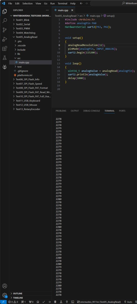
When the WhiteBoard64 is powered by 3.3V from a linear lab PSU, the results become more stable: +/- 1 LSB at 12 bit ADC resolution. These tiny variations may as well be caused by real noise in the fairly long, unshielded hookup wires, or actual fluctuations in the PSU voltage.
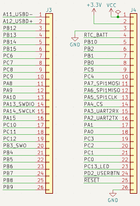
Some microcontroller pins have dual purposes. PA11 and PA12, for example, serve as D- and D+ on the USB interface. If your project involve USB connection, you must avoid other uses for these two pins. If no USB is involved, you are free to use these pins for GPIO.
Similarly, pins PA13 and PA14 are used for ST-LINK interface. If you are going to upload or debug firmware via ST-LINK, don’t use these pins for other purposes.
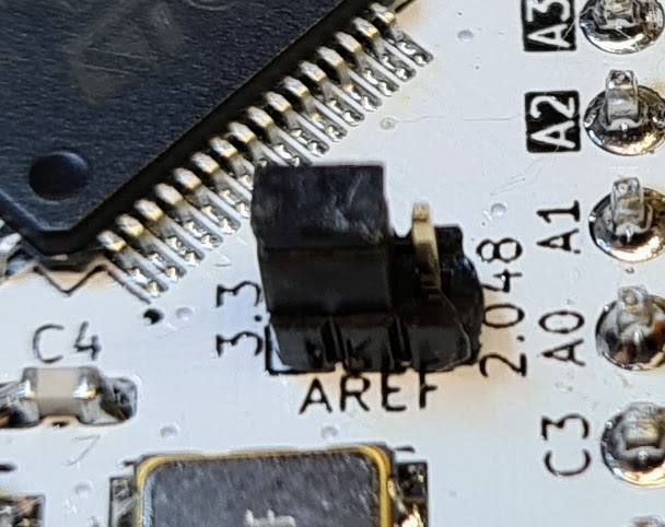
Dual-purpose pins to be aware of are emphasized with inverse (white on black) text on the board, and are labeled with double names on the schematic.

The optional FLASH memory uses SPI interface, but you can also use the same SPI pins for external devices, except Chip Select (PA4). I made two development boards, one with- and one without FLASH chip
FLASH memory code examples are provided on this project’s on GitHub repository.

Leave a comment