For microcontroller projects where you need lots of digital IO and analog inputs, an STM32 may be a good choice. The most commonly used STM32 among hobbyists is probably the basic STM32F103C8T6, known from breadboard-friendly “Blue Pill” boards, but there is a broad range to choose from. For a couple of ongoing projects, I’ll be using the STM32F411RET6, which implements ARM Cortex M4 running at 100MHz, 512kB program memory, 128kB RAM, up to 50 I/O ports of which 16 can be used as analog inputs (12 bit ADC), USB, 5 x SPI/I2S, 3 x I2C and 3 x USART, just to mention a few characteristics/features. This MCU comes in a 64-pin LQFP package, but several other packages are available.
Along with their microcontrollers, ST Microelectronics offers a range of reasonably priced development boards for demonstration and learning. To get started with the STM32F411RET6, I bought the NUCLEO-F411 development board, which has all the needed components for the MCU to work, pin headers for all MCU pins, and an integrated ST-LINK for programming and debugging. The drawbacks are board size and breadboard-unfriendliness.

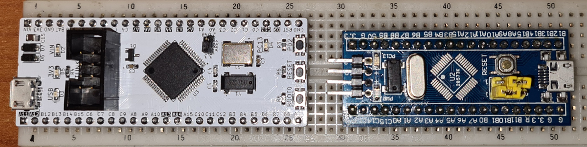
To facilitate breadboard prototyping with STM32F411RET6, I designed a compact development board, with some extra features:
- Switched voltage regulator, with wide input voltage range: 5-30VDC, low ripple, and 600mA output current.
- Selectable voltage reference for the ADC.
- Optional 32Mb (4MB) FLASH memory for e.g. data logging.
- ST-LINK interface connector (IDC8).
Some commercially available development boards have names like Blue Pill and Black Pill. Since what I designed is a board and it’s white, i decided to call it WhiteBoard64, where the number 64 reflects the number of pins of the MCU. Though being designed specifically for STM32F411RET6, this board is probably compatible with other STM32s (check datasheets for pinout).
Schematic:
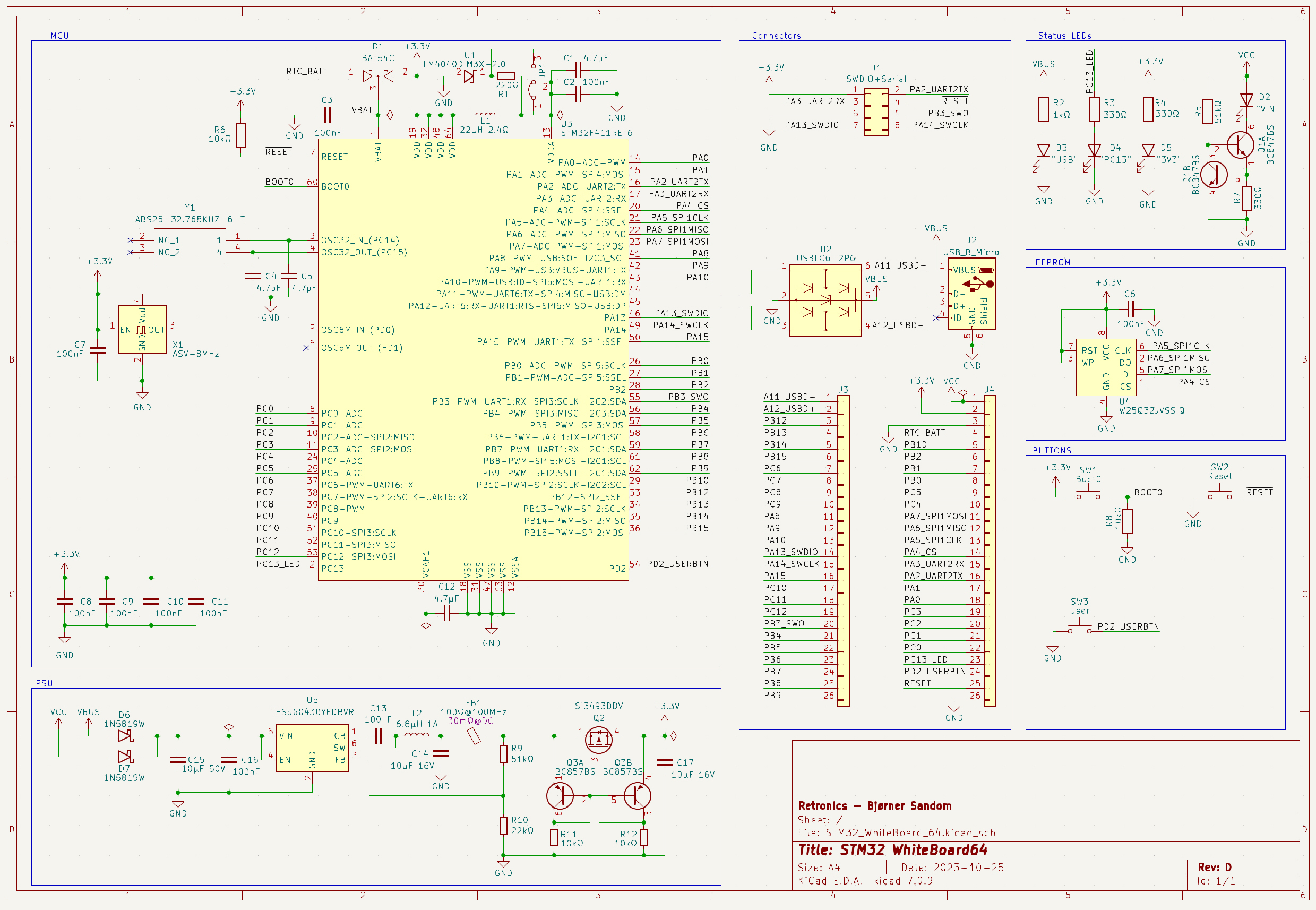
The switched voltage regulator is based on a quite new buck converter from Texas Instruments: TPS560430YFDBVR, which allows up to 36V input, adjustable output voltage, and up to 600mA current draw. This buck converter comes in different variants, but the one with letters YF after the numbers, has a switching frequency of 2.1MHz, which allows a small inductor to be used, and Forced PWM to achieve low ripple. I added som extra filtering on the 3.3V output, and a reverse current protection circuit (Q2 and surrounding circuitry), to allow the 3.3V pin on the board to be used as both input (for driving the board from an external 3.3V PSU), and as output for driving peripherals like displays and sensors.
For its main clock frequency, the STM32F411RET6 allows resonators/oscillators of different frequencies to be used. Some internal magic (PLL) scales this up to 100MHz. I’ve chosen a 8MHz oscillator. The 32.768kHz resonator is typically used for real-time clock. When a battery (1.65-3.6V) is connected to the BAT pin, the RTC keeps track of time while the MCU is switched off.
The ADC needs a voltage reference to work. The WhiteBoard64 has two AREF options, selectable with a jumper:
- 3.3V from the main supply, with some extra filtering to keep this voltage as smooth as possible. This is the standard way on most development boards.
- 2.048V from a LM4040DIM3X-2.0 voltage reference. With this, variations in the 3.3V supply voltage doesn’t affect the ADC accuracy. 2.048V may seem like an odd value, but a 12 bit ADC converts the analog input voltage to a number between 0 and 4096. 2.048V/4096=500µV => each step on the scale represents a nice round value of 500µV. If the reference voltage is 3.3V, one LSB represents 805.664µV.
The USB interface can be used for both firmware upload and emulating USB devices like for example a keyboard or mouse. When programming STM32s, I do, however, prefer to use an ST-LINK adapter, and the WhiteBoard64 has a port for this. In addition to SWDIO/SWCLK etc., one UART interface is made available through this port, to enable commands like Serial.print() to be used via the ST-LINK to show debug info or other data on the IDE console (called Serial Monitor in Arduino IDE), if you’ve got an ST-LINK adapter which supports this. The cheap ones you get from online marketplaces apparently do not, but those who are included with Nucleo boards do. I made an interface board for the Nucleo ST-LINK, for quick and easy connection with 8-pin IDC or FFC cables.
An optional W25Q32JVSSIQ FLASH memory chip, with SPI interface, can store 4MB of data. Other FLASH chips with the same package and pinout will probably also work.
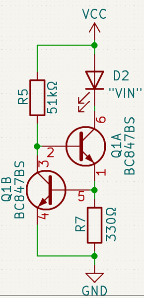
3 LEDs show whether 3.3V, USB voltage (5V), and VIN (5-30V). The circuit to the left is a constant current regulator which makes the LED shine at a constant brightness over the whole input voltage range.
Functionality of the RESET button is pretty obvious, while the BOOT0 pin is used for firmware upload via USB: hold down BOOT0 while hitting RESET. This starts the MCU in DFU mode.
In addition, there is one LED connected to MCU pin PC13 and one button connected to PD2. Use these for whatever you want.
Most STM32 pins are directly available through pin headers along the sides of the board.
PCB design:

I managed to route all the tracks on a two layer board, for economical reasons. PCB manufacturers like JLCPCB offer a very low price for small 2-layer boards, but the price increases with more layers. Some may argue that the lack of dedicated power and GND layers can affect EMI and high frequency performance, but this is after all a development board designed for use with solderless breadboards, and the breadboard and hookup wires will be the limiting factor anyway.
Production files (Gerber) and KiCad design files are published to GitHub.
Continue to Part2 for assembly and testing.

Leave a comment